- 您现在的位置:买卖IC网 > Sheet目录1214 > EVAL-ADE7880EBZ (Analog Devices Inc)BOARD EVAL FOR ADE7880
�� �
�
�The� ADE7880� supports� a� fully� licensed� I� C� interface.� The� I� C�
�ADE7880�
�I� 2� C-Compatible� Interface�
�2� 2�
�interface� is� implemented� as� a� full� hardware� slave.� SDA� is� the�
�data� I/O� pin,� and� SCL� is� the� serial� clock.� These� two� pins� are�
�shared� with� the� MOSI� and� SCLK� pins� of� the� on-chip� SPI�
�interface.� The� maximum� serial� clock� frequency� supported� by� this�
�interface� is� 400� kHz.�
�The� two� pins� used� for� data� transfer,� SDA� and� SCL,� are� configured�
�in� a� wire-AND’ed� format� that� allows� arbitration� in� a� multimaster�
�system.�
�The� transfer� sequence� of� an� I� 2� C� system� consists� of� a� master� device�
�initiating� a� transfer� by� generating� a� start� condition� while� the� bus�
�is� idle.� The� master� transmits� the� address� of� the� slave� device� and�
�the� direction� of� the� data� transfer� in� the� initial� address� transfer.� If�
�the� slave� acknowledges,� the� data� transfer� is� initiated.� This�
�continues� until� the� master� issues� a� stop� condition,� and� the� bus�
�becomes� idle.�
�Data� Sheet�
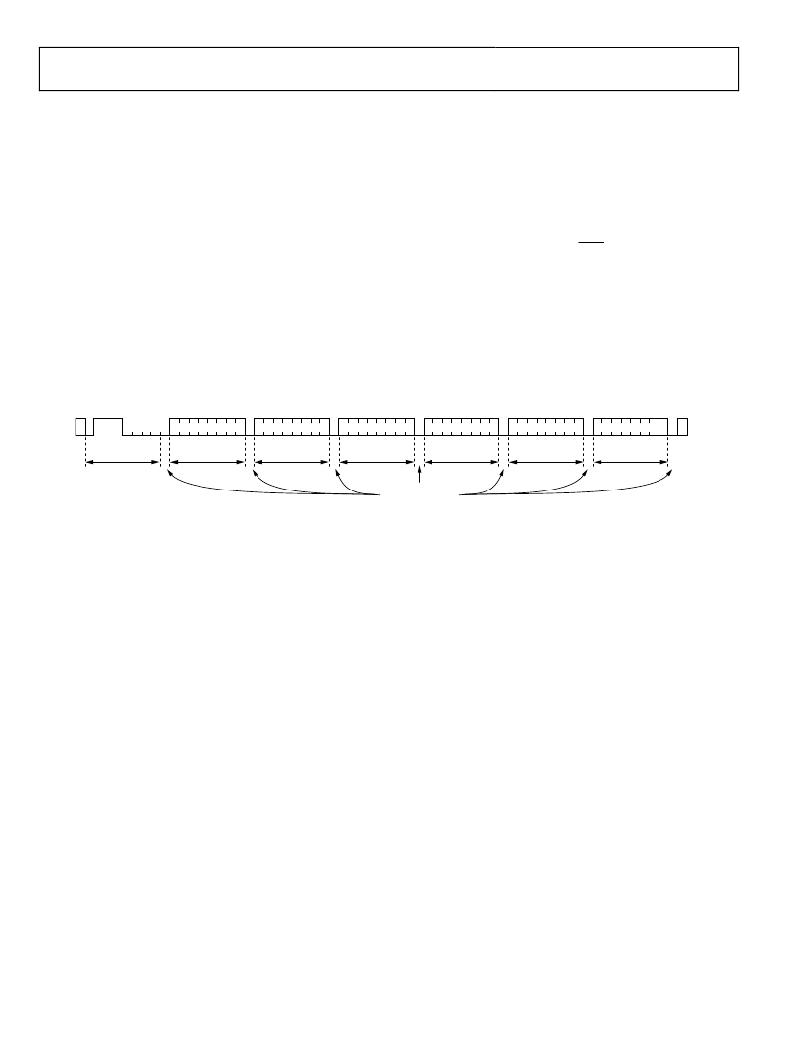
�I� 2� C� Write� Operation�
�The� write� operation� using� the� I� 2� C� interface� of� the� ADE7880�
�initiate� when� the� master� generates� a� start� condition� and� consists�
�in� one� byte� representing� the� address� of� the� ADE7880� followed�
�by� the� 16-bit� address� of� the� target� register� and� by� the� value� of�
�the� register.�
�The� most� significant� seven� bits� of� the� address� byte� constitute�
�the� address� of� the� ADE7880� and� they� are� equal� to� 0111000b.�
�Bit� 0� of� the� address� byte� is� a� read/write� bit.� Because� this� is� a�
�write� operation,� it� has� to� be� cleared� to� 0;� therefore,� the� first� byte�
�of� the� write� operation� is� 0x70.� After� every� byte� is� received,� the�
�ADE7880� generates� an� acknowledge.� As� registers� can� have� 8,� 16,�
�or� 32� bits,� after� the� last� bit� of� the� register� is� transmitted� and� the�
�ADE7880� acknowledges� the� transfer,� the� master� generates� a�
�stop� condition.� The� addresses� and� the� register� content� are� sent�
�with� the� most� significant� bit� first.� See� Figure� 100� for� details� of�
�the� I� 2� C� write� operation.�
�15�
�8�
�7�
�0�
�31�
�24�
�23�
�16�
�15�
�8�
�7�
�0�
�S� 0� 1� 1� 1� 0� 0� 0� 0�
�S�
�SLAVE� ADDRESS�
�MOST� SIGNIFICANT�
�8� BITS� OF� REGISTER�
�ADDRESS�
�LESS� SIGNIFICANT�
�8� BITS� OF� REGISTER�
�ADDRESS�
�BYTE� 3� (MOST�
�SIGNIFICANT)�
�OF� REGISTER�
�BYTE� 2� OF� REGISTER�
�BYTE� 1� OF� REGISTER�
�BYTE� 0� (LESS�
�SIGNIFICANT)� OF�
�REGISTER�
�ACK� GENERATED�
�BY� ADE7880�
�Figure� 100.� I� 2� C� Write� Operation� of� a� 32-Bit� Register�
�Rev.� A� |� Page� 74� of� 104�
�发布紧急采购,3分钟左右您将得到回复。
相关PDF资料
EVAL-ADE7953EBZ
BOARD EVAL FOR ADE7953
EVAL-ADF4002EBZ1
BOARD EVAL FOR ADF4002
EVAL-ADG788EBZ
BOARD EVALUATION FOR ADG788
EVAL-ADM1021AEB
BOARD EVAL FOR ADM1021
EVAL-ADM1023EB
BOARD EVAL FOR ADM1023
EVAL-ADM1031EB
BOARD EVAL FOR ADM1031
EVAL-ADM1062TQEBZ
BOARD EVALUATION FOR ADM1062TQ
EVAL-ADM1075CEBZ
BOARD EVAL FOR ADM1075
相关代理商/技术参数
EVAL-ADE7880EBZ
制造商:Analog Devices 功能描述:ADE7880, ENERGY METER, 3 PH, SPI, I2C, E
EVAL-ADE7913EBZ
制造商:AD 制造商全称:Analog Devices 功能描述:3-Channel, Isolated, Sigma-Delta ADC with SPI
EVAL-ADE7953EBZ
功能描述:BOARD EVAL FOR ADE7953 RoHS:是 类别:编程器,开发系统 >> 评估演示板和套件 系列:- 标准包装:1 系列:PSoC® 主要目的:电源管理,热管理 嵌入式:- 已用 IC / 零件:- 主要属性:- 次要属性:- 已供物品:板,CD,电源
EVAL-ADF4001EBZ2
制造商:Analog Devices 功能描述:Evaluation Board For Pll Frequency Synthesizer 制造商:Analog Devices 功能描述:ADF4001 PLL SYNTHESIZER EVAL BOARD
EVAL-ADF4002EB1
制造商:Analog Devices 功能描述:EVAL BOARD - Bulk
EVAL-ADF4002EBZ1
功能描述:BOARD EVAL FOR ADF4002 RoHS:是 类别:编程器,开发系统 >> 评估演示板和套件 系列:- 产品培训模块:Obsolescence Mitigation Program 标准包装:1 系列:- 主要目的:电源管理,电池充电器 嵌入式:否 已用 IC / 零件:MAX8903A 主要属性:1 芯锂离子电池 次要属性:状态 LED 已供物品:板
EVAL-ADF4007EBZ1
功能描述:BOARD EVALUATION FOR ADF4007EB1 RoHS:是 类别:编程器,开发系统 >> 评估演示板和套件 系列:- 标准包装:1 系列:PSoC® 主要目的:电源管理,热管理 嵌入式:- 已用 IC / 零件:- 主要属性:- 次要属性:- 已供物品:板,CD,电源
EVAL-ADF4106EB1
制造商:Analog Devices 功能描述:PLL, Frequency Synthesizer